
Introduction
Vision
Two forms of embedding are considered here:
-
Formed components, where the PCB dielectric and conductive traces are key elements themselves in the components, e.g., formed resistors, mmWave antennas, and optical waveguides.
-
Embedded components where the components can be passive discretes or integrated active components. Interconnections with the PCB can be wirebond, bumps or direct die attached. The cavities housing embedded components can be open or closed (link to Appendix).
Embedded technologies combine components, assembly and packaging processes in a single manufacturing facility. The organization of supply chains is a critical challenge.
The key benefits of embedding components in PCBs, in comparison with conventional PCB attachment, include:
-
Miniaturization—Embedding components like resistors, capacitors, and ICs directly into the PCB substrate reduces the overall package size, which is crucial for compact and high-density designs
-
Improved Electrical Performance—By embedding components, the electrical path lengths are minimized, reducing parasitic effects such as capacitance and inductance. This enhances signal integrity and reduces noise and interference, especially in high-frequency applications. Similarly improved power distribution network performance can be achieved.
-
Thermal Management—Embedded components allow for innovative thermal solutions, such as integrating thermal vias or cores within the PCB. This helps dissipate heat more effectively, ensuring reliable operation in high-power applications
-
Reliability—Reducing the number of solder joints and external interconnections improves the overall reliability of the package, making it suitable for demanding applications like aerospace and medical devices.
-
Cost Efficiency—While the initial manufacturing process may be complex, embedding components can reduce the need for additional packaging and assembly steps, leading to long-term cost savings.
Table 1 focuses on the core aspects of embedded PCB components:
Table 1. Embedded PCB Component Overview
|
Component Type |
Description |
Key Characteristics |
Typical Uses |
Advantages of Embedding |
|
Embedded Resistors |
Resistors integrated within the PCB layers using resistive materials. |
|
|
|
|
Embedded Capacitors |
Capacitors formed within the PCB layers using dielectric materials. |
|
|
|
|
Embedded Inductors |
Inductors created using conductive traces within the PCB layers. |
|
|
|
|
Embedded Integrated Circuits (ICs) |
IC chips that are placed within cavities at PCB internal layers. |
|
|
|
|
Embedded Thermal Vias |
Vias designed specifically to transfer heat away from components within the PCB. |
|
|
|
Applications
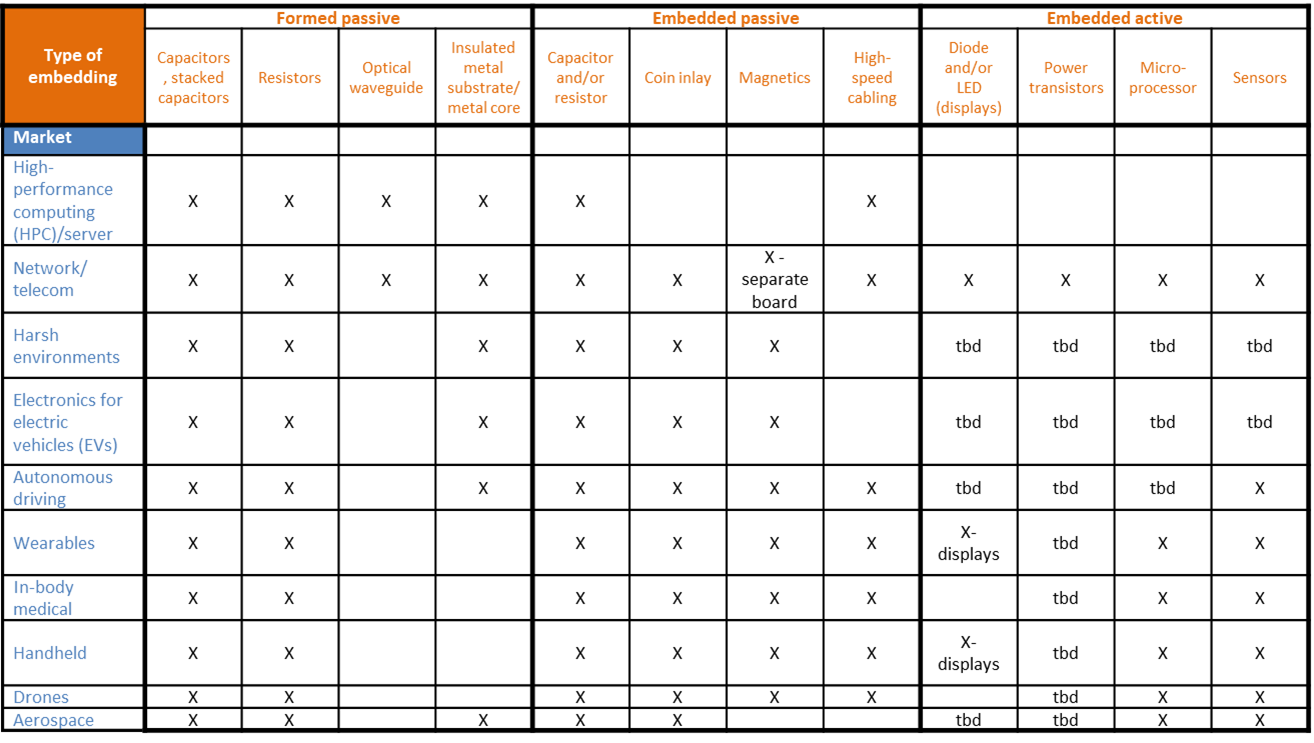
Due to their benefits, embedded components can be exploited in a wide range of applications. See Table 2 for a mapping of the types to components to various types of electronic systems.
Table 2. Existing and emerging embedded landscape applications
Drivers and Challenges
As can be seen from the key application domains highlighted in Table 2, the drivers for embedding and in-PCB formed components are
(a) smaller form factors, particularly for low-profile applications,
(b) reduced material costs and ecological footprint, and
(c) reduced power and signal losses, especially at high data rates and high frequencies.
The latter two drivers arise from reduced lengths for leads and connectors and the reduction/elimination of device packaging.
In meeting these drivers, several technical challenges emerge, as follows:
The cost and time adder of advanced materials development and selection:
-
Developing materials that support higher speeds and better reliability.
-
Innovations in substrates and laminates.
-
Improving surface finish to minimize losses at higher frequencies.
The technical limits of manufacturing:
-
Implementing precise manufacturing processes, probably with new manufacturing equipment, to ensure higher yield and reliability through repeatability in volume runs.
-
Survivability of embedded assemblies at processing temperatures, similar to concerns in traditional board assembly, without impairing functionality.
-
Overcoming assembly challenges in and around cavities, with ultra-thin and flexible PCBs.
Rigorous testing:
-
Developing new testing routines to ensure embedded components meet performance standards.
-
Addressing the complexities of testing at higher frequencies.
Scalability and cost reduction for embedded electronics:
-
Enhancing scalability of production techniques, including adding new equipment.
-
Finding cost-effective solutions for mass production.
Artificial intelligence (AI) and automation in manufacturing:
-
Manufacturing and assembly of PCBs with embedded components will follow the same path as heterogenous integration in advanced packaging, with increasing adoption and integration of AI and automation. Integrating AI and automation into existing manufacturing processes will require significant investment in new technologies and training. Additionally, the amount and variety of data and its precision increases dramatically with embedded components, increasing the challenge for customized AI solutions.
Sustainable manufacturing practices:
-
Cost implications: Implementing eco-friendly manufacturing practices can involve higher upfront costs, which may be a barrier for some manufacturers. The end result of embedding, however, is lower material use due to the implicit miniaturization of leads and connections.
Ultimately, widespread adoption of embedded electronics in high-volume manufacturing will happen after either:
a) Driven by more exacting functional requirements, key original equipment manufacturers (OEMs) invest in the supply chain to support new high-volume applications with embedded electronics or
b) Equipment suppliers seed the market with the required manufacturing equipment line-ups.
Needs, Gaps, Challenges and Potential Solutions
Controlling the formation of PCBs with embedded components involves addressing a series of processing issues. These issues are discussed further at the following links: (a) for formed passives, (b) placed passives and (c) placed active components. (Note for reviewers: See Appendices B, C and D.) The resulting roadmaps of needs gaps, challenges and potential solutions are given in Table 3 and Table 4 below.
Technology Status Legend
For each need, the status of today’s technology is indicated by label and color as follows:
|
In-table color + label key |
Description of Technology Status |
|---|---|
|
Solutions not known |
Solutions not known at this time |
|
Solutions need optimization |
Current solutions need optimization |
|
Solutions deployed or known |
Solutions deployed or known today |
|
Not determined |
TBD |
Table 3. Embedded Components- Needs, Gaps, and Today’s Technology Status with Respect to Current and Future Needs
|
|
ROADMAP TIMEFRAME |
|||
|
TECHNOLOGY ISSUE |
TODAY (2025) |
3 YEARS (2028) |
5 YEARS (2030) |
10 YEARS (2035) |
|
TECHNOLOGY ISSUE #1: DESIGN |
||||
|
ISSUE 1A-Guidelines and standardization of design (depends also on process tech choice) Standardization transition determined by competition |
||||
|
NEED |
Transitions from guidelines to standards |
Standardization of design rules |
Further expansion of standardization |
|
|
CURRENT TECHNOLOGY STATUS |
Few players dominant, industry not mature/little competitiveness so barrier to adoption |
|||
|
GAPS |
Available supplies, e.g., capacity and availability of supplier base |
Available supplies, e.g., capacity and availability of supplier base |
|
|
|
CHALLENGES |
|
|
Evolution of component types and competing solutions (optical versus embedded versus others) |
|
|
ISSUE 1B-Design dependency on supplier’s manufacturing line-up and know-how |
||||
|
NEEDS |
|
Assessments based on design thresholds to reduce variability influencing designs for fine feature sizes and frequencies, to inform guidelines and design rules (depends on JEDEC) |
||
|
CURRENT TECHNOLOGY STATUS |
Limited availability of information from fabricators and sub-supplier (line up and know how) (e.g., material parameters) for clarity and granularity of design models |
|||
|
GAP |
Lack of capability of fabricators/suppliers to deliver (Resistors are limited by size, based on sheet resistance) |
|||
|
CHALLENGES |
|
|||
|
ISSUE 1C-Improved support in design tools (third party tool versus in-line tools) |
||||
|
NEED |
Tools for embedded designs that include testability and are compatible with existing Gerber trusted data transfer software that is exportable with importable material properties (computer-aided design (CAD)/computer-aided manufacturing (CAM)) |
Wide-spread adoption of tools that evolve for embedded designs that include testability and are compatible with existing Gerber trusted data transfer software that is exportable with importable material properties (CAD/CAM) |
Wide-spread adoption of tools that evolve for embedded designs that include testability and are compatible with existing Gerber trusted intelligent data exchange software that is exportable with importable material properties (CAD/CAM) |
Wide-spread adoption of tools that evolve for heterogeneous integrated (HI) embedded designs that include testability and are compatible with existing Gerber trusted intelligent data exchange software that is exportable with importable material properties (CAD/CAM) |
|
CURRENT TECHNOLOGY STATUS |
Limited use, not widely distributed – to be optimized, esp. material properties |
Tools exist more widely, electrical CAD (eCAD) capabilities extended to CAD including design for X (DfX) with specialized suites and modules |
Practice and guidelines allow for more adoption due to original device manufacturer (ODM)/OEM push and data management systems |
PCB and packaging developers, manufacturers and suppliers are more aligned and technology opportunity more available for CAD |
|
GAPS |
Intellectual property (IP) – material data is limited (e.g., master parts list, variability in data and testing) |
Limited knowledge with upstarts for design requirements |
|
|
|
CHALLENGES |
Cost to implement |
|
Process capability and constrained physical interface resolutions (delamination issues) |
Slow adoption and cost prohibition due to miniaturization solutions that exist today and are not fully exhausted Risk assessment |
|
ISSUE 1D-Design for manufacturing (e.g. CAD v. CAM) |
||||
|
NEED |
Maturity is needed beyond definitions of guidelines for CAD/CAM transitions, e.g., IPC 7092-A1 |
Adoption of newly matured guidelines for CAD/CAM |
||
|
CURRENT TECHNOLOGY STATUS |
Few PCB embedded companies (not widespread) as suppliers to large companies Embedded MOSFET companies/suppliers few |
|||
|
GAPS |
|
|||
|
GAP |
|
Embedded die versus components. Large, leading edge companies develop their own solutions, not sharing. |
||
|
CHALLENGES |
|
|
Complexity of evolving designs for new architectures and materials, and process technologies (e.g., optical, combinations of subtractive /additive/ embedded, etc.)
|
|
|
TECHNOLOGY ISSUE #2: PROCESS |
||||
|
ISSUE #2A-Process precision/registration (Discreet/SiPs) |
||||
|
NEEDS |
|
Alignment critical for finer feature sizes within layers, thickness tolerances for each layer/inner layers/inner laminates, based on ultra high-density interconnect (UHDI) investments |
Alignment critical for finer feature sizes within layers, thickness tolerances for each layer/inner layers/inner laminates, based on UHDI investments |
|
|
CURRENT TECHNOLOGY STATUS |
Small scale manufacturing.
|
Process optimization for UHDI |
||
|
GAP |
Lack of assembly capability and commitment in all PCB shops |
|
|
|
|
CHALLENGE |
Further investment |
|
|
|
|
NEEDS |
|
Continued improvement with:
|
Continued evolution |
Continued evolution with expanded, accelerated automation with new facilities |
|
CURRENT TECHNOLOGY STATUS |
Optimization is needed for board design, component type, processing and supply chain maturation |
Automation and AI-assisted smart manufacturing leads to adaptive success |
||
|
GAP |
|
Lack of standards for cutting edge registered outlines |
|
|
|
CHALLENGES |
|
|
|
|
|
ISSUE #2B-Process chemistries compatibilities (up and downstream in process) |
||||
|
NEED |
Upper limit to operational temperatures set by other factors, e.g., thermal dissipation in single vias for power distribution, not embeddeds. |
Increased upper limit to operational temperatures of various stack-ups, e.g., organic substrates, to accommodate the thermal load of embeddeds |
||
|
CURRENT TECHNOLOGY STATUS |
Solutions known |
Solutions need optimization |
||
|
GAP |
|
Lack of materials for higher relative thermal index (RTI) |
||
|
CHALLENGES |
|
|
||
|
NEED |
Compatibility of the system in package (SiP) with laser drilling used for attach. |
Lower cost laser drilling compatible with SiP embedding at higher volumes. |
Laser drilling with higher precision/smaller feature size |
|
|
CURRENT TECHNOLOGY STATUS |
Solution need optimization |
Solution need optimization |
Solutions unknown |
|
|
GAPS |
Capability of laser drilling to meet tight tolerances. Currently driven to expensive UHDI solutions |
Dual-UV lasers with high energy control to prevent damage to the SIPs; only with limited availability today (i.e., high cost). |
New laser technology |
|
|
CHALLENGES |
|
High precision at a low cost-point, including equivalent advances for test and verification equipment. |
||
|
ISSUE #2C-Surface real estate, breakout region |
||||
|
NEED |
PCB definition is 30-30-50 linewidth/ space /via
|
PCB definition is 20-20-40 linewidth/ space /via
|
PCB definition is 15-15-30 linewidth/ space /via
|
PCB definition is 15-15-30 linewidth/ space /via
|
|
NEED |
Cavities and alignment/registration in Z axis (placement, attachment, and connection) |
Cavity technologies solutions at inflection point for balance of investment and physical limits for miniaturization, performance at higher speed and frequencies |
Adoption to mainstream production for embedding active components into cavities with new innovations |
|
|
CURRENT TECHNOLOGY STATUS |
Solutions need optimization |
Solutions not known |
||
|
GAPS |
|
|
|
|
|
CHALLENGES |
|
|||
|
CHALLENGES |
|
|
||
|
NEED |
Interconnect geometries and interfaces’ reliability at smaller pitches (pad-to-pad, line-to-line) |
|||
|
CURRENT TECHNOLOGY STATUS |
Micro-via technology in use |
Optimization of existing materials and equipment |
No known solutions |
|
|
GAPS |
|
|
||
|
CHALLENGES |
|
|
||
|
CHALLENGE |
|
|
Metrology methods, tolerances, and equipment to be developed/adopted (defects are percentages of the feature sizes…)(Proprietary solutions exist in some cases) |
|
|
NEED |
Alignment precision refinement for specific process and flows (e.g., laser drilling, cavity drilling, etc.) |
Precision improvement for accuracy by process / methods evolution |
Evolution to adaptive inline equipment to address/handle product/process variability |
Adoption of adaptive inline equipment to address/handle product/process variability |
|
CURRENT TECHNOLOGY STATUS |
Solutions need optimization |
|||
|
GAPS |
|
|
|
|
|
CHALLENGES |
Small pitches and HDI /UHDI makes precision more difficult |
|
||
|
NEED |
For low-volume manufacturing: Volumetric registration (Z axis) reproducibility (includes IPC cavity type [1,2,3], pick and place, attachment) |
For high-volume manufacturing:
|
||
|
CURRENT TECHNOLOGY STATUS |
Solutions known |
Solutions need optimization |
||
|
GAP |
|
|
High investment and risk |
|
|
CHALLENGES |
|
|
||
|
NEED |
Copper plating for complex 3D shapes within cavities, with limited cavity aspect ratios |
Additive options for copper plating for complex 3D shapes within cavities and higher cavity aspect ratios |
More precise additive options for copper plating for complex 3D shapes within cavities |
|
|
CURRENT TECHNOLOGY STATUS |
Solutions need optimization |
Solutions need optimization |
||
|
GAPS |
High equipment cost and fabrication /facility investment |
Dedicated lines needed for these applications with higher cavity aspect ratios |
||
|
CHALLENGES |
|
|
|
|
|
TECHNOLOGY ISSUE #3: RELIABILITY |
||||
|
ISSUE #3A-Dielectric breakdown versus materials and thinness |
||||
|
NEED |
1200V/mil (automotive/power supply applications with 2mil thickness) |
2000V/mil (automotive/power supply applications with 2mil thickness) |
||
|
CURRENT TECHNOLOGY STATUS |
Solutions available
|
Solutions need optimization |
||
|
GAP |
|
|
Limited availability of high-performance materials, from power electronic devices solutions |
|
|
CHALLENGE |
|
|
Adapting for PCB manufacturing processes |
|
|
ISSUE #3B-Thermal-mechanical properties including modulus and CTE mismatch (lead joint stability) especially with hybrid materials (when coins and filled vias are used) |
||||
|
NEEDS |
|
Multifunctional / compromise of encapsulants’ properties across complex/ different components, e.g., accommodates a broader range of materials and bigger sizes |
||
|
CURRENT TECHNOLOGY STATUS |
Solutions need optimization |
No known solutions
|
||
|
GAPS |
|
|||
|
CHALLENGES |
|
|||
|
ISSUE #3C-Electrostatic Discharge (ESD) |
||||
|
NEED |
Manage machine ESD within production lines for protection of embedded SIPs |
|||
|
CURRENT TECHNOLOGY STATUS |
Solutions need optimization |
|||
|
GAP |
Many PCB manufacturing facilities not up for this – need to invest in a facility designed to manage ESD |
|||
|
CHALLENGES |
|
|||
|
ISSUE #3D-Electromigration |
||||
|
NEED |
Standards and test methods for various applications and components (e.g., mobile versus harsh environment, etc.) |
|
||
|
CURRENT TECHNOLOGY STATUS |
Solutions need optimization |
|
||
|
GAP |
Lack of harmonization of PCB and embedded standards/test methodologies |
|
||
|
CHALLENGES |
|
|
||
|
TECHNOLOGY ISSUE #4: MATERIALS |
||||
|
NEED |
Low fragmentation capable materials for better defined images |
New structural registration materials needed |
Materials for 2.5D processes for recessed components |
|
|
CURRENT TECHNOLOGY STATUS |
Solutions need optimization |
Solutions need optimization |
Solutions deployed |
|
|
GAPS |
Process is stamp and mechanical to form cavities: Limited to specific shapes (limited to imperfect squares/rectangles (no rounded corners)
|
Photo-imageable polyimide and precise materials are emerging to create needed flexibility in cavity shape. However, compatible methods/materials for laser ablation process are needed. |
Licensing |
|
|
CHALLENGES |
Co-design/co-development needed with “coin” and “embedded” technologists/ suppliers |
Equipment development |
Sharable technology for HVM |
|
|
NEED |
Resolve the low CTE mismatch of materials to [1] bridge the end product harsh environments and [2] resolve incompatibility with larger components |
Resolve the low CTE mismatch to [1] bridge the end product harsh environments and [2] resolve incompatibility with larger components with tighter bump pitch and more connections (I/O) to keep pace with ASICs |
Evolve materials and refine processes for better compatibility and connections with more supplier options |
|
|
CURRENT TECHNOLOGY STATUS |
Solutions available |
Solutions need optimization |
||
|
GAPS |
Volume manufacturing limited to smaller, thinner devices with limited/less lifecycle demand |
More automated manufacturing and robotic utilization needed, with less harsh chemicals and bonding processes
|
Higher volume in more sectors |
|
|
CHALLENGES |
|
|
||
|
TECHNOLOGY ISSUE #5: TEST CONSIDERATIONS (e.g., test types, methods/procedures, equipment) |
||||
|
NEED |
In-circuit testing (ICT) customized for ability to test embedded components |
More adoption at volume |
||
|
CURRENT TECHNOLOGY STATUS |
Solutions need optimization |
Solutions need optimization |
||
|
GAPS |
|
|
||
|
CHALLENGES |
Merging of assembly with test |
|
||
|
NEED |
New testing procedures/ equipment for embedded, integrated circuits to mimic and adopt product/device specific testing from semiconductor mfg. and end-item |
Support for transition from high-volume products to a broader range of products with low volumes and/or lower margins |
Standardization and maximization of methods (e.g., MOM, MES) (Joint industry standard for normalization (e.g., JEDEC, IEEE, etc.)) |
|
|
CURRENT TECHNOLOGY STATUS |
Solutions need optimization |
Solutions need optimization |
Solutions need optimization |
|
|
GAPS |
Limited in practice inline |
Gradual adaptation of test and capacity of sub-test suppliers and speed of replication by “followers” |
|
|
|
CHALLENGES |
|
|
|
|
|
NEED |
Functional (Parametric) Test |
Defacto understanding of data exchanges for parametric testing |
Mature, successful exchange of data among users and suppliers |
|
|
CURRENT TECHNOLOGY STATUS |
Limited to in-house, at low-volume |
Solutions to be optimized, based on emerging cooperation for data sharing |
Solutions to be optimized, and standards developed |
|
|
GAPS |
|
|
|
|
|
CHALLENGES |
Communication and data sharing among partners: ODMs/foundries and outsourced semiconductor assembly and test (OSATs), OEMs manufacturing defect analyzer (MDA) and failure analysis (FA) feedback for improvement |
Data sharing balance among users and suppliers
|
|
|
|
NEED |
Functional (Parametric) Test - Equipment available with PCB fabricators |
Equipment to be broadly available with PCB fabricators |
||
|
CURRENT TECHNOLOGY STATUS |
Solutions available |
|||
|
GAP |
Fabricators will need to understand the test equipment previously only with PCBA |
|||
|
CHALLENGES |
Test much more complex at this level, as compared to bare board. Learning/experience lacking. |
Equipment investment costs. |
||
|
ISSUE #6: CLEANROOMS’ CLASS COMPLIANCE (CERTIFICATION) |
||||
|
NEED |
High cleanliness (Class 100 cleanroom) on panel edges/cut surfaces |
Class 100 adopted by mainstream HVM |
||
|
CURRENT TECHNOLOGY STATUS |
Solutions need optimization |
|||
|
GAPS |
Class 10000 overall (Class 1000 for imaging).
|
Investment in cleanroom builds and automation and feedback control/monitoring |
|
|
|
CHALLENGES |
|
|
|
|
|
ISSUE #6A-Control of process residues’ contamination for PCB, assembly-level, and environmental particulates (operating environment)) |
||||
|
NEEDS |
|
High frequency applications (56GHz) will push for support for embedding in high-speed PCB, with associated clean-room requirements. |
Increased automation to reduce manual handling, allowing a broader range of PCB manufactures to support bare-die embedding. |
|
|
CURRENT TECHNOLOGY STATUS |
Solutions need optimization. |
|||
|
GAP |
Limited to manufacturers with stringent environmental controls, e.g. substrate providers. |
|||
|
CHALLENGES |
Higher requirements with bare die handling. |
Expanding the industry capacity. Investment costs and ensuring ready availability of trained/certified staff. |
||
Potential Solutions
Table 4 considers approaches to address the above needs and challenges. The evolution of these is projected out over a 10-year timeframe using technology readiness levels (TRLs).
|
In-table color key |
Range of Technology Readiness Levels |
Description |
|---|---|---|
|
2 |
TRL: 1 to 4 |
Levels involving research |
|
6 |
TRL: 5 to 7 |
Levels involving development |
|
9 |
TRL: 8 to 9 |
Levels involving deployment |
Table 4. Embedded Components Potential Solutions
|
|
|
EXPECTED TRL LEVEL* |
|||
|
TECHNOLOGY ISSUE |
POTENTIAL SOLUTIONS |
TODAY (2025) |
3
(2028) |
5
(2030) |
10
|
|
#1 DESIGN |
Maturation of CAD services (including electrical testability rules, e.g., shorts) and general design rules. |
5 |
6 |
7 |
8 |
|
|
Maturation of guidelines for design for assembly (DFA) combined with DFM (for module-type control) building on IPC 7092 |
5 |
6 |
7 |
8 |
|
|
Technology co-optimization techniques in design |
5 |
6 |
7 |
8 |
|
#2 PROCESS |
Compatible chemistries broad availability and experience |
4 |
5 |
6 |
7 |
|
|
Laser ablation optimization with better equipment |
6 |
7 |
8 |
8 |
|
|
Thermo-mechanical process impact optimization |
5 |
6 |
7 |
8 |
|
|
Expansion of available technology for electrostatic (ESD) control (infrastructure and on manufacturing lines) |
5 |
6 |
7 |
8 |
|
|
Electrostatic over stress (EOS) control |
5 |
6 |
7 |
8 |
|
|
Improved clean-room specifications from PCB debris/poor process control: board assembly, operator-level |
5 |
6 |
7 |
8 |
|
|
Reduced contamination by use of robotics within production line |
5 |
6 |
7 |
8 |
|
|
2.5D to 3D printing transition and more MSAP to deal with finer features |
5 |
6 |
7 |
8 |
|
|
Dielectric control – i.e., printables (inkjet, e.g., for lead parasitics reduction) for size limitation arising from sheet resistance |
5 |
6 |
7 |
8 |
|
#3 RELIABILITY |
Material selection matches end-product operational and environment consideration (acceptable moisture-related levels) |
6 |
7 |
8 |
8 |
|
|
Merging of advance packaging and laminate (PCB) with DFR knowledge and experience |
5 |
6 |
7 |
8 |
|
|
Library for chipsets, dies, and materials’ properties for component and encapsulation levels |
5 |
6 |
7 |
8 |
|
|
Improved design practices for thermo-mechanical property control for embedded die and more advanced applications |
6 |
6 |
7 |
8 |
|
|
Electrostatic (ESD) control for products |
6 |
6 |
7 |
8 |
|
|
Harmonized (PCB versus embedded components) standards and test methods for electromigration and other reliability concerns (IPC 7092) |
7 |
8 |
9 |
9 |
|
|
Optimized materials and processes for dielectric control and dielectric property control (higher withstand voltage for polymers, etc.) |
6 |
7 |
8 |
9 |
|
|
Matching conductive via fill for Tg and CTE of the laminate material |
6 |
7 |
8 |
9 |
|
#4 MATERIALS |
Low-fragmentation materials for Type 2 cavities |
7 |
8 |
9 |
9 |
|
|
Substitution by substrate-type materials to give low or controlled (z-axis) CTE mismatch |
6 |
7 |
8 |
9 |
|
|
Encapsulation materials that can be baked in – no prepreg |
6 |
7 |
8 |
9 |
|
|
Better knowledge-base and understanding of embedded module testing for high-volume manufacturing (HVM), low-margin and specificity by component type |
5 |
6 |
7 |
8 |
|
#5 TEST |
Optimized testing solutions like semiconductor and PCB practices for embedded, discrete components |
5 |
6 |
7 |
8 |
|
|
Software to support modules for functional parametrics |
5 |
6 |
7 |
8 |
|
|
Automated “Test and Trim” capability for formed resistors |
5 |
6 |
7 |
8 |
|
|
Cross-over/combined bare-board testing and ICT for active embeddeds |
5 |
6 |
7 |
8 |
Conclusions
The key gaps that need to be addressed by the PCB manufacturing industry include:
-
Design and Simulation: The Need for Smarter Software
Current design for manufacturability (DFM) and for assembly (DFA) algorithms are often treated separately and too generic, lacking the necessary support for embedding technologies, especially in low-volume applications. OEMs must encourage electronic design automation (EDA) software providers to enhance embedding-specific design rules, process constraints, and simulation capabilities to better support embedded PCB technologies. -
Material Selection: Addressing CTE Mismatch and Thin Structures
CTE mismatch between embedded components and dielectric materials can lead to stress-related failures. Additionally, as PCB designs become thinner, controlling defects and warpage in multi-layer embedded structures becomes increasingly complex. Choosing low-CTE, high-reliability materials will be essential for long-term performance. -
Manufacturing: The Role of Advanced Process Control
To ensure high production yield and consistency, process control must evolve to advanced automation for precise layer-to-layer and X,Y - registration. This includes real-time data collection and automated process control to optimize manufacturing conditions and high-precision handling equipment to support delicate, thin multi-layer build-ups, including large role-out of AI for optimization. -
Manufacturing: The Role of Advanced Equipment. The integration of AI and advanced 3D printing offers new opportunities for embedded component processing that were not previously available. Further investment in these processes will potentially accelerate the adoption of embedded components, as both become more available.
-
Testing and Qualification: Rethinking Traditional Methods
The qualification and approval process for embedded PCBs remains a bottleneck, as it often takes too long compared to standard PCB technologies. The industry must shift towards functional testing of completed modules, integrating it within the PCB fabrication process at a reasonable cost. Additionally, as electrical testing evolves, there will be a greater emphasis on functional verification rather than traditional in-circuit testing. This must include burn-in tests to ensure product reliability.
Defect detection in embedded PCBs is more challenging than in conventional designs, particularly for active components. The industry standard organizations must develop effective inspection and testing methodologies.
-
Scaling Up: Overcoming Cost and Standardization Barriers
Scaling up involves not only increasing production volumes but also adapting the technology to different board form factors, applications and dedicated facilities. Standardization is needed across the supply chain to ensure compatibility between different PCB manufacturers, material suppliers, and assembly houses. That will support cost reduction strategies, including process efficiency improvements and material optimizations. -
Workforce Development: Building Expertise for Next-Generation Manufacturing
The transition to embedded PCB technology requires a skilled workforce capable of managing advanced process control, material science, and design optimization. Training programs should focus on process management and supervision, particularly in areas like ESD control and high-precision component handling. Cross-disciplinary expertise combining PCB fabrication knowledge with semiconductor-level process control is also needed (e.g. initiatives like ESDA from Semi [1]). Cross-industry knowledge transfer would feed-up and to ensure a smooth industry-wide transition. -
The Shift Toward PCB and Semiconductor Processes Merging
As embedded PCB fabrication is evolving towards mass production the industry is moving closer to semiconductor manufacturing practices, for example more advanced cleanroom control, more ESD protection in production, and the capability for finer feature resolutions. This transition presents new opportunities for semiconductor equipment providers to develop specialized tools for high-precision embedding, testing, and packaging.
PCB Acronyms
References
-
JPCA, JPCA PWB Technology Roadmap, 2023.