Cloud & High-Performance Computing Application Requirements for Advanced Packaging
Basic drivers
The variety and intensity of processing workloads for cloud, edge and local computing is continually increasing. This places unprecedented demand on processors, communications and the electronics hardware systems that host these.
The major trends that have a critical impact on the electronics hardware include:
Increasing processing density along with an increasing variety of processor architectures needed to solve more complex tasks. Cloud computing has evolved from a single-size-fits-all general-purpose processors to graphical processor units to machine-learning training and inference engines. The efficiency gains afforded by specialization is just one response to a voracious appetite for increased processing power. The other response is to simply increase the density of compute power.
The demand for communication throughput has similarly increased. This occurs at all levels, from rack to board, from board to packaged device, from packaging to chip, from chip to chip. Speed increases for long-distance wireless and wireline communication are simply a proxy for similar increases at all levels.
The power consumption for these processing and communication loads is projected to increase dramatically. This is a critical parameter due to the resulting increases in operational costs for users and in environmental costs due to carbon emissions. Higher power consumption also implies higher heat dissipation and a knock-on effect on reliability.
Design for security will come to the forefront of device architecture design. Concerns include prevention of (a) side-attacks through information leakage at the interposer or via on-board power regulators and (b) denial-of-service (DoS) and side-attacks through chiplet proximity.
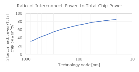
Figure 1: Chiplet-scale power trend; source: [1].
Architecture Vision
The combined challenges of increased processing workloads, higher data throughput demands and spiralling energy impacts is driving the following architecture paradigms:
Parallelism. The continued march towards fine-grained parallelism challenges scalability in processor devices. Memory coherence and interconnect bottlenecks will limit algorithmic performance. Power efficiency at low workloads will also be a concern.
Process in memory. Many emerging cloud applications have very heavy demands on memory bandwidth to and from the processor cores. These include:
Deep neural networks (DNNs) and homomorphic encryption (HE) workloads in AI solutions
Transaction processing
Database applications
Search
This is leading to architectures built around the “processing-in-memory” paradigm where memory and processing are co-designed into the same core.
Increased use of 3D stacking. Again, to minimize demands on interconnect and the associated power consumption, 3D stacking will be more extensively used. However, this will be limited by the challenges of power distribution and heat extraction.
More radical architecture innovations. For specialized applications, more radical architectures may prove successful. Low-power, noise-tolerant applications may open up opportunities for analog AI accelerators based on analog multiply-and-accumulate (MAC) units. Others have proposed and prototyped large wafer-scale systems that may find niche uses.
Key Technical Attributes
How do these trends map to critical parameters in PCB and packaging design and their underlying technologies?
Processing
Here the main parameters are as follows:
The choice of chip technology is a key determinant of processing density and even can impact the ease of implementation of the processor architecture.
The limits of vertically stacking and the horizontal distribution of stacks or chips distributed horizontally are the other key parameters for the processing density.
The choice of chip size impacts the efficacy of the workload partition and distribution.
See Table 1 below for some insights into how some of these parameters need to evolve over time.
Table 1: Key attribute needs related to processing for cloud and HPC applications.
Attribute/parameter | Units | Need | |||
Today (2023) | 2026 | 2028 | 2033 | ||
Substrate size | mm x mm | 74 x 74 | 100 x 100 | 115 x 115 | 140 x 140 |
Number of stacked dies |
| Processor on top or alone in stack-up | Processor on/near top with DRAM, voltage regulation, etc. underneath; low # of layers | ||
HBM stacking – fast followers |
| 8 dies + microbumps | |||
HBM stacking – lead edge |
| 12 dies + microbump | 16 - hybrid bonding | ||
Interconnect
The data throughput either into a packaged device or into a chip is a relatively simply function, i.e. the product of the per-lane speed and the number of pins/communication lanes. The latter is inversely proportional to square of the pin pitch and, of course, directly proportional to the package or chip size.
See Table 2 below for the expected evolution of these parameters. Note that connector or bump size is generally about 50% of the connector pitch. While minimum pitch distance represents a key bottleneck, increasing use of designs with mixed bump pitches also are challenging from a manufacturing perspective.
Table 2: Key attribute needs related to device connectivity for cloud and HPC applications.
Attribute/parameter | Units | Need | |||
Today (2023) | 2026 | 2028 | 2033 | ||
Architecture | |||||
Board architecture |
| Fly-over cabling, on-board optics | Near-chip optics to reduce Cu trace-length and power consumption | ||
Board architecture (mainstream) |
| PCB + face-plate optics | Fly-over cabling + on-board optics | ||
Connector pitch | |||||
Package pin pitch | mm | 0.95-1.00 | 0.9 | 0.85 | 0.7-0.8 |
Standard solder bumps | µm | 130 to 150 |
| 100 | |
Micro bumps | µm | 50 to 30 |
| 20 | |
RDL | µm | 25 |
|
| 10 |
Cu-Cu Hybrid Bond | µm | 20 | 10 | ||
Parallel bus | |||||
Signal Speed per Lane |
| 32 Gb/s | 64 Gb/s | 128 Gb/s | Not Known |
Protocol | PCIe Gen5, NRZ | PCIe Gen6, PAM-4 | PCIe Gen7, PAM-4 | PCIe Gen8+, PAM-16 | |
Application example |
| NVM Storage | Not known | Not known |
|
Serial interfaces | |||||
Signal speed per pair | Gb/s | 112 Gb/s | 112 Gb/s | 224Gb/s | Not Known |
Protocol | 400GbE, PAM-4 | 800GE, PAM-4 | 1.6TbE, PAM-4 | 3.2TbE, PAM-16 | |
Application |
| Data Center NIC | Data Center NIC | Data Center NIC |
|
It should be noted that at the package level, the desired processor capability no longer is the bottleneck, but the data communication requirements are. This is because radical decreases in pin pitch are not anticipated and lane speeds are increasing at a relatively sedate pace as compared to demands on communication throughput.
Power
Total power consumption can be broken down into three different elements:
Power consumption of processing (including memory usage)
Power consumption of communications/interconnect
The power needed to drive the thermal management solution
The first two components depend directly on the PCB, packaging and die technologies. The increases in both are driving changes in the power delivery architecture.
The third drives the choice of the overall thermal management architecture, which in turn has knock-on impacts on both PCBs and packaging.
Table 2: Key attribute needs related to power and thermal management for cloud and HPC applications.
Attribute/parameter | Units | Need | |||
Today (2023) | 2026 | 2028 | 2033 | ||
Thermal design power from the hottest package
| Watts | 700 | 800 | 1000 | 1300 |
Thermal design power from the hottest package
| Watts | 400 | 600 | 800 | 1000 |
Max current per device | A | 400 | 600 | 800 | 1000 |
Thermal design flux (package) | W/sq. cm | 10 | 15 | 20 | 25 |
Thermal design flux | W/sq. cm | 100 | 150 | 200 | 250 |
Cooling Method | type | Air cooling + cold plate for GPU/CPU | Assisted air cooling + cold plate for GPU/CPU | 2-phase liquid cooling in the cold plate | Immersion cooling |
References
Semiconductor Research Organization, MAPT: 2023 Interim Report, 2023.