Packaging & Heterogeneous Integration
This is a brief overview of the topic Packaging & Heterogeneous Integration. To avoid duplication, many links here point to specific sections in MAPT, the NIST-supported Microelectronics and Advanced Package Technologies Roadmap and, to a lesser extent, to HIR, the Heterogeneous Integration Roadmap.
iNEMI’s own roadmapping efforts focus on assembly and packaging processes.
Vision
Challenging application requirements are putting more stress on key functions of system-in-package (SIP) devices. Increasing data rates challenge connectivity; higher currents, the power delivery subsystem; and miniaturization, the choice of substrate and thermal management technologies.
To respond to this, substrates in SIPs have had to evolve from being a physical carrier to a system integration platform. As more and more diverse functionality is packed in, technology heterogeneity is another challenge for the industry. These challenges have to be addressed throughout the product lifecycle, from design to assembly to test, with a complex system integration (CIS) approach being the only way forward.
Scope
This page summarizes key findings from other roadmaps1,2 and work3, particularly MAPT, across many of the critical dimensions:
Architecture and interconnection (including a novel approach to categorizing advanced packaging architectures)
In a few key areas, iNEMI provides its own perspectives:
Key Applications
New and growing application areas that depend on advances in packaging and heterogeneous integration include the domains listed below. These in turn provide the critical requirements that shape those advances.
High performance computing
See here for the expected evolution in packaging-related requirements arising from high performance computing, including AI processing and cloud computing.
Other critical applications
Harsh environments like those presented to automotive drive train applications lead to higher ambient temperatures combined with higher reliability requirements. New, highly compact applications with optics, such as AR/VR are forcing photonics/electronics integration in to the one package. Applications such as 5G handsets and basestations and ADAS (automated driving assistance systems) depend on low-loss, low-dispersion propagation and processing of mmWave signals.
If you are interested in contributing to an iNEMI-led initiative in this space or just wish to be informed when that initiative has results to publish, please click here.
Architecture and Interconnection
With the mass adoption of heterogeneous integration as a means to achieve functional scaling, the architecture of SIPs has become increasingly complex and across the various applications, extremely diverse.
The lack of a broadly accepted nomenclature has also added to the confusion. For the purposes of roadmapping packaging architectures, we adopt D.C. Hu’s taxonomy3 for the needs here. See Figure 1 for the common die-to-die stacking approaches and Figure 2 for the common interposer-to-laminated-substrate connectivity options. For further discussion of this nomenclature, including mappings to various commercial offerings please see [4].
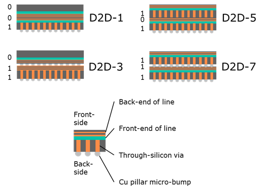
Figure 1: Nomenclature for basic die-to-die stacking architectures.3
Table 1: Die-to-die architecture tag scheme.
Tag | Structure a/b/c | Orientation |
|---|---|---|
D2D-1 | 0/0/1 | Face-to-face |
D2D-3 | 0/1/1 | Face-to-face |
D2D-5 | 1/0/1 | Back-to-back |
D2D-7 | 1/1/1 | Back-to-back |
a = TSV (through-silicon via) for top die, yes (1) or no (0) | ||
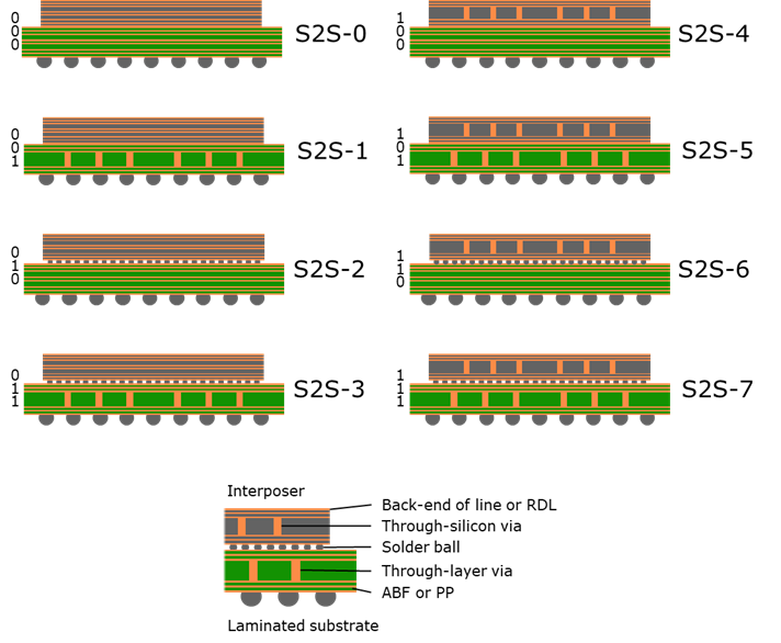
Figure 2: Nomenclature for basic substrate-to-substrate architecture options.3
Table 2: Substrate-to-substrate stacking architecture scheme
Tag | Structure a/b/c |
|---|---|
S2S-0 | 0/0/0 |
S2S-1 | 0/0/1 |
S2S-2 | 0/1/0 |
S2S-3 | 0/1/1 |
S2S-4 | 1/0/0 |
S2S-5 | 1/0/1 |
S2S-6 | 1/1/0 |
S2S-7 | 1/1/1 |
a = TLV (through-layer via) for top substrate, yes (1) or no (0) | |
There is an on-going trend from via-centric architectures to via-less and from micro-bumps to hybrid copper bonding techniques. So for example, in inter-substrate connectivity we are seeing a transition from S2S-7 architectures to S2S-3, S2S-1, and S2S-0 architectures.3 This is the result of the two trends from connection technologies identified in MAPT: ever reducing pitch and energy per bit, supporting ever-increasing data transfer rates.
For further insights into the evolution of the connectivity supported between dies, interposers, and substrates, see Section 7.3 of the MAPT Roadmap.
Substrate Technology
The role of substrates is evolving beyond a simple physically carrier of IC dies and other devices. Substrates are becoming a key part of the overall hardware system integration, providing both connectivity and power delivery. Increasing demands for both, from major emerging applications, are driving advances in packaging substrate technology.
These advances are covered in Section 7.6 of the MAPT Roadmap.
Materials
Increased package size, reduced feature size, increasing signalling rates and bandwidths, increased power delivery and operating temperatures—all depend heavily on material properties. Potential evolutionary paths of key material properties are explored in MAPT’s Tables 8.1, 8.2 and 8.3 for power electronics, mmWave applications and high-performance computing respectively.
Power Delivery
As the number and diversity of devices within a single package increases, there is a commensurate increase in the number of power rails and of voltages supplied. Increased miniaturization, especially in low-profile mobile packages, leaves less room for the inductors and capacitors needed for voltage conversion.
Section 7.4 of MPAT provides an overview of the evolution of IVR (integrated voltage regulator) architectures, enabling power delivery solutions with fewer voltage rails to the package, each at at higher voltages. Tables 7.2 gives the the roadmap for this architectural evolution and other technology requirements.
Thermal Management
Chiplet power density is increasing; 3-D stacking is becoming more prevalent; dies and their constituent layers are becoming thinner—these all lead to thermal hotspots becoming smaller and more intense. High-speed I/O power consumption is also increasing. Thermal management materials and technologies need to evolve to address these drivers.
Design complexity for thermal management hardware solutions is also dramatically increasing due to (a) heterogeneity of heat generation within a package; (b) increased use of package-level thermal management hardware and (c) coupling of thermal management design and (electronics) hardware architecture design.
Table 7.3 in MAPT explores the evolution of the technologies and design methodologies for advanced package thermal management solutions.
Design
Design of SIPs is challenging, given the inherent 3D nature of the solution; the mixed domains of different chiplets; the lack of standardized or common libraries for chiplets, interposers, packages and their interfaces; and indeed, the sheer variety of technology and architecture choices.
Table 9.2 in MAPT outlines the key investment areas needed to address these challenges, over a 15-year time frame.
Modelling
Comprehensive modelling of SIPs imply a suite of models that span up to 8 orders of magnitude in physical dimensions and are inherently multi-modal to account for the different technologies used and the interplay between function, mechanics, thermals, etc. MAPT’s Table 7.6 details the modelling needs.
Assembly
To achieve the ever-increasing level of functionality needed in SIPs, significant advances in assembly and packaging-related processes are needed. Some consideration has been given in other roadmaps, e.g. Section 7.7 in MAPT, but a more detailed roadmapping effort is needed.
If you are interested in contributing to an iNEMI-led initiative in this space or just wish to be informed when that initiative has results to publish, please click here.
Test
Test functionality that once was achieved at the board level, increasingly has to be provided at the SIP level. Functional testing with a “bed-of-nails” approach has to achieve the same test coverage with a highly integrated package. Further, unlike a traditional PCB, the layout is increasingly 3D rather than 2D. Even as test compression reaches it limits, reduced opportunities for test access points implies additional pressure on speed of connections supporting test data extraction.
For a discussion on the implications at the system level, please see Testability/In-Field Reliability for CIS. For discussions on the implications of heterogeneous integration and advanced packaging, see Section 10, Chapter 17 in the HIR Roadmap.2
Reliability and Metrology
Application-specific reliability requirements are mapped out in MAPT’s Table 7.7. As discussed in Section 7.8, advanced packaging solutions involve new materials, structures and assembly techniques while packing ever more functionality into smaller volumes. Ensuring reliability meets the requirements is challenging.
A first step is to ensure that the appropriate metrology is in place, meeting needs as outlined in Table 10.2. The underlying challenges are discussed in Section 10.8, while the likely evolution of metrology techniques is presented in Table 10.1.
References
Semiconductor Research Organization, MAPT: Microelectronics and Advanced Packaging Technologies Roadmap, https://srcmapt.org/wp-content/uploads/2024/03/SRC-MAPT-Roadmap-2023-v4.pdf, 2023.
IEEE EPC, Heterogeneous Integration Roadmap, https://eps.ieee.org/technology/heterogeneous-integration-roadmap.html, 2024.
Dyi-Chung Hu, “Substrate 2.0 for the Future AI Servers“, IMPACT 2023 – International Microsystems, Packaging, Assembly, and Circuits Technology Conference, 27 Oct. 2023.
INEMI, “A Common Nomenclature for Substrate and Die Integration in Advanced Packaging,” INEMI Technical Note, December 2024.