Integrated Photonics
The demand for highly integrated photonics solutions is growing due to the need for high-speed communications and high-performance computing hardware to support applications such as ultra-high-definition video streaming, social networking, metaverse, automated logistics, and artificial intelligence (AI). Analysts have projected that the revenue for data communications optics (co-packaged optics/on-board optics, active optical cables and embedded optical modules, and Ethernet) will be $15.1B in 2026 and grow to $28.1B by 20321.
During this growth period the fiber optics hardware will evolve from pluggable transceiver optics, to on-board optics, followed by co-packaged optics, and finally leading to optical I/O, which will enable the optical engine and application-specific IC (ASIC) to be physically placed closer together. This fiber optics evolution will improve signal integrity and increase bandwidth while reducing the interconnect electrical path and the energy consumed per bit transferred.
The CIS toolbox will enable the optics product designers to select the appropriate materials, structures, assembly processes, and testing tools to address several challenges: interconnect pitch, redistribution layer (RDL) line/space, high power/heat dissipation, warpage, and reliability. In addition, CIS services providers will be able to consolidate the supply chain and co-locate the capabilities required to manufacture the optics products, thereby reducing the risk and final cost to the customer. A CIS manufacturing site may offer several critical capabilities, such as:
Post-CMOS processes—Cu pillar bumping, under bump metallization (UBM), oxide etching, KOH V-groove, etc.
Wafer-level assembly—Chip-on-wafer (CoW) process, wafer-level (WL) wirebond, high precision optical placement, etc.
Wafer-level test — Wafer sorting, WL optical test and burn-in, etc.
Module assembly — SMT process, flip chip assembly, encapsulation, fiber attachment, etc.
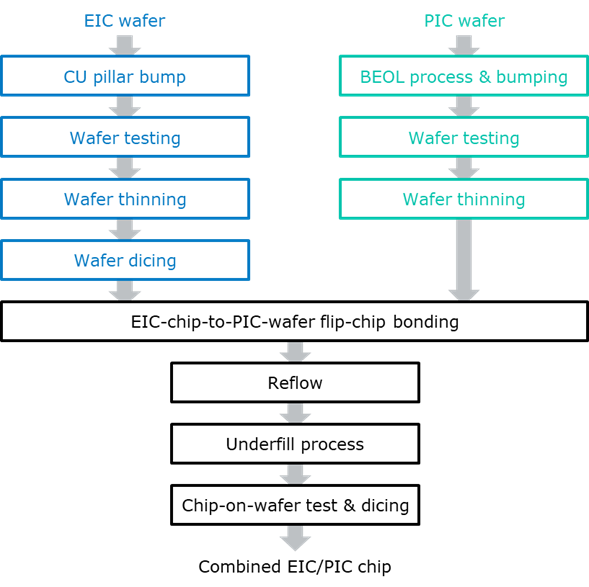
Locating the capabilities in one facility can enable a more resilient supply chain providing an efficient manufacturing process flow. One example of such a manufacturing process, for a CoW optics structure, is shown in Figure 1.

Figure 1. Example of the manufacturing process flow for a chip-on-wafer optical structure.
Effective cleaning processes are necessary to maintain the purity and integrity of silicon photonics devices, ensuring optimal performance and reliability for applications such as data transmission and sensing. Contaminants can introduce defects, alter optical properties, and cause signal attenuation or loss, thereby degrading the efficiency and accuracy of photonics components.
Return to topic overview
References
Yole, https://www.yolegroup.com/.
