Complex Integrated Systems
Introduction
Moore’s Law and monolithic implementations
For much of the latter half of the last century, the evolution of electronics was focused on increased digitization and miniaturization. This was implemented using a homogeneous implementation fabric—digital processing on silicon. Moore’s Law ensured that viable economics and performance targets could be met. Even today, work continues on this concept with further reductions in feature size and integration of new functionality on-chip (e.g., silicon photonics).
Beyond Moore and system-in-package
Further reductions in on-chip feature size have become ever more costly as the basic physics has limited further easy gains. The concept and practice of “heterogeneous integration” – different functions implemented on different implementation fabrics – has been adopted throughout the industry. Each fabric is optimized for the needs of a small set of similar functions. Those fabrics (often separate die) are integrated into a single package (system-in-chip).
The approach has benefits in better power efficiency, smaller implementations, and sometimes simpler processes. To take advantage of the better yields and easier handling of smaller dies, even homogeneous functions such as memory are now split across multiple die and vertically stacked in a single package.
Redefining packaging
The system-in-package (SiP) concept can also be limiting. Recently, concepts and implementations that eliminate or redefine the role of the package have emerged. Direct attach of bare die to module-sized substrates, have eliminated traditional packaging in some 5G mobile handset processor modules. Use of antenna-in-package for mmWave systems redefines the role of the package, adding functional requirements. High-speed printed circuit boards (PCBs) are increasingly being implemented as substrates.
Complex integrated systems
Complex integrated systems (CIS) combine different types of functions—e.g., digital, analog, optical, micro-mechanical, power-related, structural—in a single system to ensure the best solution fit for the product and its end market. These are systems where:
For any given function, the specialized implementation technology and/or material system that provides the best performance at the right cost point is chosen.
The different function implementations are integrated using the most appropriate interconnect and packaging solutions.
Multiscale, holistic approaches are essential for design, simulation, assembly and test across the complete, sustainable product lifecycle, including manufacturing.
The resulting supply chains intelligently integrate the capabilities, expertise, and business practices used across wafer fabrication, chip/die packaging, module assembly and final system assembly.
CIS products are designed by leveraging a rich portfolio of active components, structural elements, and functional materials such as:
Optics—CMOS, lens, mirror, displays
Photonics—Photonic IC (PIC), fiber, light emitting diode (LED)
Electronics—passive, active, integrated, printed
Mechanics—enclosures, motors, servos, micropumps
Substrates—rigid, flexible, stretchable
Materials—electrical, thermal, optical, mechanical
Sensors
SiP devices, heterogeneous integration, and chiplets are just one set of possible integrations for CIS solutions. Other highly integrated assemblies also come in under the definition of CIS, including direct attach to rigid and flexible substrates, mixed optical/electrical assemblies, compact sensor modules, etc.

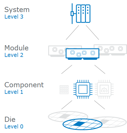
Figure 1. The multiple possible levels of CIS integration.
As shown in Figure 1, CIS can involve integration of multiple lower layer hardware components to a higher-level unit, starting from wafer to components to modules to systems. It is important to note that software and networking are not considered here.
Scope
The scope is set mainly by the definition of CIS above. The rest of this topic is organized as follows:
Key applications that are enabled by CIS are discussed in some detail.
The implications for the organization of the electronics manufacturing ecosystem are explored.
The impacts on the major facets of the full product lifecycle are discussed.
Technical needs, gaps, challenges and solutions are outlined.
List of recommendations for individual firms and the electronics industry ecosystem are provided.
Applications
Even today, there are some significant CIS applications in the marketplace, e.g. personal devices such as smart watches and hearing aids, high-end SiP solutions for compute and graphical processing, etc..
However many new critical applications that are now scaling into mass adoption require even further integration across a wider range heterogeneous technologies. These new market opportunities are then the critical drivers for complex integrated systems. In aggregate, the market opportunities associated with CIS solutions have significant annual growth rates and companies are investing tens of billions of dollars to address these opportunities.
Sample applications that require CIS include:
High-Performance Computing Applications in Edge Devices and Data Centers
Augmented reality/virtual reality/mixed reality (AR/VR/MR) Devices
CIS Ecosystem—Blending Manufacturing Verticals
The manufacturing ecosystem for CIS will see significant changes in supply chain roles.
The assembly of CIS-enabled products requires a combination of different processes, tools, and equipment that have traditionally existed in different electronics manufacturing verticals (wafer foundry, outsourced semiconductor assembly and test (OSAT), and electronics manufacturing services (EMS)). In the past companies were hesitant to extend or change their role in the value chain due to the inherent barriers to entry (e.g., capital expenditure (CAPEX), operational expenditure (OPEX), manufacturing facilities, etc.). These barriers no longer present a concerning risk profile for companies considering CIS services because demand has increased and manufacturing revenues are growing at attractive, sustainable rates.
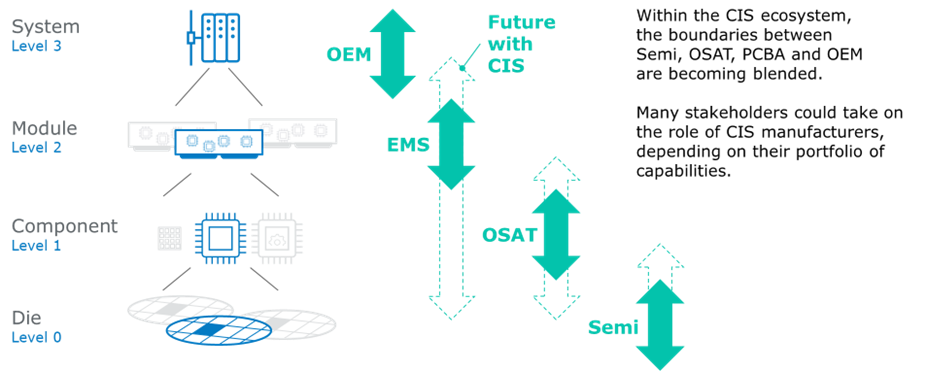
This blending of roles in CIS supply chains is illustrated in Figure 2. Different players may become dominant through vertical integration in different market segments. Consolidation is likely due to savings arising from increased efficiency and accountability. However, it is challenging to predict the shape of new supply chains due to the tensions between technology investments needed; the degree of product mix for given market segments, and the margins available.

Figure 2. Blending of roles within the CIS supply chain.
Companies that offer CIS design engineering and manufacturing services have acquired the necessary capabilities and equipment from the different verticals, thereby offering complete product assembly at one facility. This provides the customer with the most secure and efficient supply chain. The following list of processes—which in the past would have been available at companies representing multiple manufacturing verticals—can now be found at a single CIS services company:
Wafer-to-wafer bonding, die-to-wafer bonding
Wafer thinning
Wafer, panel and die handling
Wafer probe and test
Interconnects/bumping
Precision placement
Micro-dispensing
Artificial intelligence (AI)-enabled active alignment
Wire bonding
Handling/placement of electro-optical, electromechanical, semiconductor devices,
Encapsulation, evaporation, plasma, nanocoating
Surface mount technology (SMT), higher level assembly (HLA), final assembly test and packaging (FATP)
In addition, supply-chain management for CIS needs to include tight quality control of input components, e.g., in terms of technical cleanliness. The logistics for assembly of the CIS product minimizes the handling and shipping of unfinished modules from location to location, thereby minimizing supply chain disruption and reducing the product carbon footprint.
Impacts on the Complete Product Lifecycle
Any quick survey of the needs and challenges shows that realization of products as CIS is much more than just technologies for integrating previously separate components. Full lifecycle support is needed, from design to manufacture to test. Serious investment is needed, in people, infrastructure, and processes.
Consider each element within the product lifecycle, as follows:
Technical Needs, Gaps and Solutions
The technology issues surrounding CIS, the associated needs, technology status of those needs, as well as gaps and challenges to overcome, are summarized below. The time period considered is from 2024 to 2034.
For each need, the status of today’s technology is indicated by label and color as follows:
Table 1: Color key for technology status
In-table color + label key | Description of Technology Status |
|---|---|
Solutions not known | Solutions not known at this time |
Solutions need optimization | Current solutions need optimization |
Solutions deployed or known | Solutions deployed or known today |
Not determined | TBD |
Table 2. CIS Needs, Gaps, and Today’s Technology Status with Respect to Current and Future Needs
| ROADMAP TIMEFRAME | |||
TECHNOLOGY ISSUE | TODAY (2024) | 3 YEARS (2027) | 5 YEARS (2029) | 10 YEARS (2034) |
CIS application: Compact analog transceivers for 5G mmWave systems | ||||
NEED | Integrated analog mmWave solutions including antenna | Integrated mmWave solutions including beam-shaping antenna | ||
CURRENT TECHNOLOGY STATUS | Solutions deployed or known | Solutions not known | ||
GAP | Low-loss reconfiguration | |||
CHALLENGE | Reducing mmWave propagation losses in packaging technology | Many switching components are highly non-linear and lossy | ||
CIS application: Power efficient power amplifiers for 5G mmWave systems | ||||
NEED | Low-profile thermal management for power amplifiers (PAs) | Minimized PA connection distance to rest of transceiver chain | ||
CURRENT TECHNOLOGY STATUS | Solutions known | Solutions need optimization | ||
GAP | None—embedded Cu coins are used for easy heat extraction | Lack of mmWave design tools to support embedding of active devices (e.g., PA die) in substrates/PCBs | ||
CHALLENGE | Lack of experience combining materials and tolerances needed of mmWave applications with embedding technologies for PCB and substrates. | |||
CIS application: High-performance computing (HPC) applications in edge devices and data centers | ||||
NEED | Advanced PCB manufacturing capabilities - please see PCB roadmap | |||
NEED | Manufacturing and assembling for large package size | |||
CIS application: High precision micro-lens alignment and placement in AR/VR headsets | ||||
NEED | Multiple alignment steps via optical active alignment | Optimization of quality metrics | Address expensive BOMs for cost sensitive markets | Optical active alignment a standard process (i.e., SMT) |
CURRENT TECHNOLOGY STATUS | Solutions need optimization | Solutions need optimization | Solutions need optimization | Technology status not determined |
GAP | Long cycle times | Placement not optimal due to lack of key performance indicators (KPI) feedback | Components are not commodities yet | |
CHALLENGE | Multiple discrete steps require longer cycle times than traditional (passive alignment) methods | Development and optimization of algorithms to be done by entities that have experience of all parts of the ecosystem (i.e., software (SW), hardware (HW), manufacturing processes of micro-optics, and opto-mechanical systems). | Miniaturized high performance optical modules have not gained critical mass or reached their full market potential.
| Technology adoption, standardized design, and manufacturing processes are required to make this technology available and cost effective. |
Heterogeneous integration and chiplets | ||||
NEED | Different chip architectures and technologies for different processing functions. Smaller die with high yields in production and reliability in use | Standardization of interfaces and form factors of chiplets/chips within a single package | Diversification with heterogeneous wafer/die-level technologies (e.g., introduction of GaAs/III-V die with CMOS die), including supply chain diversification. | |
CURRENT TECHNOLOGY STATUS | Solutions need optimization | Solutions need optimization | Solutions not known | |
GAP | Incomplete reliability data for packages with chiplets. | Some interconnect standards (e.g., the Universal Chiplet Interconnect Express (UCIe)). Physical design standards such as 3Dblox specify the description date, but not form factors. | Reduced interconnect pitch (<1 um), allowing easy integration of functions from different die, without power or area penalty. Ultra-thin die (<10 um) needed. | |
CHALLENGE | Lack of solder/joint reliability data. | Some industry organization needed | ||
Design for CIS: Increasing power efficiency of closely coupled member and logic | ||||
NEED | Normalized designs for optimized close coupling of memory and logic/compute | Standardization and design techniques for optimized close coupling of memory and logic/compute | Fast system design tools for efficient power delivery and thermal management | |
STATUS | Solutions deployed or known | Solutions need optimization | Solutions not known | |
GAP | Evolution of JEDEC Solid State Technology Asso. (JEDEC): collaboration needed between memory and logic suppliers, with different approaches today | Go beyond chiplet integration—tighter integration at the die level | ||
CHALLENGE | Build on high bandwidth memory (HBM) stacking, with tight interconnect pitch | |||
Design for CIS: System architecture design tools | ||||
NEED | Interconnects at the deepest possible level, to simplify higher levels of integration, improving reliability and power efficiency | |||
CURRENT TECHNOLOGY STATUS | Solutions need optimization | |||
GAP | Optimal trade-off between depth of integration and specialization of the implementation for the functions integrated | |||
CHALLENGE | Improved system architecture design tools | |||
Design for CIS: Multi-domain simulation | ||||
NEED | Improved thermal management profiling in electronic design automation (EDA) tools. | Improved multi-physics EDA tools. | ||
CURRENT TECHNOLOGY STATUS | Solutions need optimization | Solutions need optimization | ||
GAP | Lack of spatial granularity in existing computational fluid dynamics/ finite element analysis (CFD/FEA) tools for CIS and silicon photonics | Improved spatial granularity/simulation speed. | ||
CHALLENGE | Characterization of materials at the micro level | Multi-scale capture for CIS. | ||
Smart manufacturing for CIS | ||||
NEED | Harmonization of protocols between equipment from chip fab to final assembly including high-precision passive alignment and active optical alignment | Equipment to support the standard, both hardware and software | Complete line integration | |
CURRENT TECHNOLOGY STATUS | Solutions deployed or known | Solutions need optimization | Solutions not known | |
GAP | Different protocols at different stages of manufacture. | Equipment supporting disparate protocols. | ||
CHALLENGE | Multiple parts of the ecosystem need to engage | Legacy equipment won’t support new standard. | ||
Workforce Development for CIS | ||||
NEED | Workforce conversant in optical and electrical technologies at system architecture level | |||
CURRENT TECHNOLOGY STATUS | Solutions need optimization | |||
GAP | Low number of capable technical experts | |||
CHALLENGE | Limited comprehension in optical CIS, particularly in the design and process of miniaturized assemblies. Multiple disciplines needed, plus understanding of system view. | |||
Table 4 considers approaches to address the above needs and challenges. The evolution of these is projected out over a 10-year timeframe using technology readiness levels (TRLs).
Table 3: Color key for technology readiness levels
In-table color key | Range of Technology Readiness Levels | Description |
|---|---|---|
2 | TRL: 1 to 4 | Levels involving research |
6 | TRL: 5 to 7 | Levels involving development |
9 | TRL: 8 to 9 | Levels involving deployment |
Table 4. Complex Integrated Systems, Potential Solutions
|
| EXPECTED TRL LEVEL* | |||
TECHNOLOGY ISSUE | POTENTIAL SOLUTIONS |
TODAY (2024) | 3 (2027) | 5 (2029) | 10 |
Compact analog transceivers for 5G mmWave systems | Antenna-on-package | 8 | 9 | 9 | 9 |
MEMS-based antenna reconfiguration | 4 | 6 | 9 | 9 | |
High precision micro-lens alignment and placement in AR/VR headsets | Independent suppliers (i.e., microelectromechanical systems (MEMS). Vertical-cavity surface-emitting lasers (VCSELs), optics, manufacturing, etc.) to work together to create a standard or guidelines | 2 | 3 | 5 | 7 |
Heterogeneous integration and chiplets | Physical standards for chiplet integration into SIP solution | 2 | 5 | 8 | 9 |
New solder alloy metallurgies for shrinking electrical connections | 3 | 5 | 8 | 9 | |
Design for CIS: System architecture design tools | Improved system design tools for complex integrated systems | 6 | 7 | 8 | 9 |
Design for CIS: Multi-domain simulation | Multi-physics EDA tools tools with improved spatial granularity and simulation speed | 6 | 7 | 9 | 9 |
Smart manufacturing for CIS | Protocol harmonization. Examples of existing protocols include the Semiconductor Equipment Communication Standard/Generic Equipment Model (SEC/GEM) (within semiconductor fabrication)2, Hermes (primarily for SMT)3, and IPC, Association Connecting Electronics Industries, IPC-2591 Connected Factory Exchange (CFX)4. | 7 | 7 | 9 | 9 |
Workforce for CIS | Address CIS in smart manufacturing and other courses | 7 | 8 | 9 | 9 |
Multi-disciplinary thinking and system design introduced in undergraduate-level technical courses | 6 | 7 | 8 | 9 | |
Recommendations
Successful design and manufacturing of CIS electronics requires new technology for miniaturization and integration. However, delivering compact integrated functionality is only part of the challenge. As discussed above, the full product lifecycle needs to be addressed, from workforce development to design and test, to end-of-life repurposing and recycling.
For individual companies, a number of actions are required:
Technology development focused on miniaturization.
Adoption of system design tools that determine the trade-offs between different technologies and integration architectures.
Adoption of design for test, for manufacturing, and for sustainability as core design principles.
Investment in new process and manufacturing capabilities, opening up new integration possibilities within a single facility.
Facility equipment and processes that accommodate both cleanroom environments of back-end of line packaging and the flexibility of board assembly capabilities.
More broadly, we call for improved CIS situation awareness and a concerted effort to build a CIS community focused on collaborative, cross-industry initiatives for realizing the following:
Standards and frameworks to support cross-supply chain traceability of materials, components, and their associated test data for CIS, building on existing standards such as IPC-17825.
Standardization of data exchange formats within CIS electronic design automation (EDA) flows.
Standardization of physical form factors and physical interfaces for chiplets.
Standardized assembly techniques to ease materials extraction for recycling and (in the longer term) component extraction for reuse.
Strong cross-technology knowledge base for designers, manufacturing engineers, test and manufacturing technicians that now need to work with multiple technologies during design and manufacture. This includes increased multi-disciplinary thinking and system design in undergraduate-level technical courses.
If the above issues are successfully addressed by the industry, then CIS electronics will have significant positive impact both on commercial opportunities for individual companies and on targeted societal challenges.
References
INEMI, IPC, “Complex Integrated Systems: The Future of Electronics Manufacturing“, whitepaper, https://go.ipc.org/complexintegratedsystems, March 2024.
SEMI, “SEMI E30 - Specification for the Generic Model for Communications and Control of Manufacturing Equipment (GEM)”, https://store-us.semi.org/products/e03000-semi-e30-specification-for-the-generic-model-for-communications-and-control-of-manufacturing-equipment-gem.
IPC, “IPC-HERMES-9852: The Global Standard for Machine-to-Machine Communication in SMT Assembly”, https://www.the-hermes-standard.info/.
IPC, IPC-2591-Version 1.7: Connected Factory Exchange (CFX), https://shop.ipc.org/ipc-2591/ipc-2591-standard-only/Revision-17/english, August 2023.
IPC, IPC-1782 - Revision A - Standard Only: Standard for Manufacturing and Supply Chain Traceability of Electronic Products, https://shop.ipc.org/ipc-1782/ipc-1782-standard-only/Revision-a/english, November 2020.

