Introduction
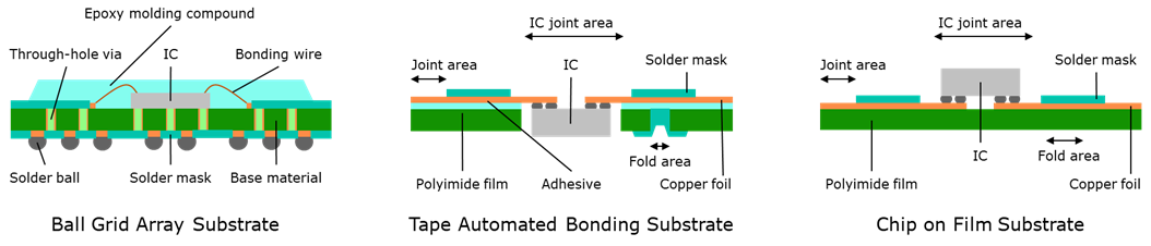
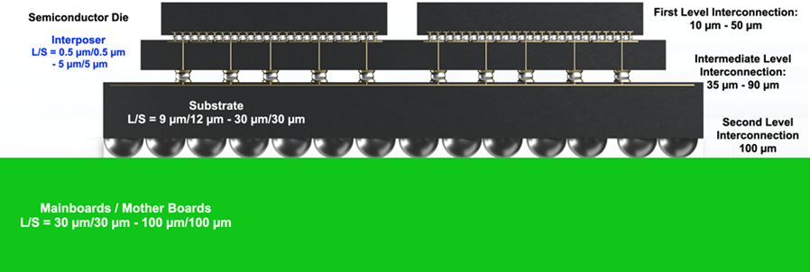
Organic substrates are widely used as carriers for semiconductor integrated circuits such as microprocessors, graphics processors, field-programmable gate arrays (FPGAs), and memories. Semiconductor package substrates can be divided into general purpose semiconductor package substrates, tape-automated bonding (TAB) carriers, and chip-on-film (COF) carriers (see Figure 1). Organic substrates are made by printed wiring board-based technologies used for semiconductor device packaging, and are separate from the choice of semiconductor package or semiconductor device type. It is also classified into interposer and substrate according to role played in a given semiconductor package (see Figure 2).
Needs, Gaps, Challenges, and Potential Solutions
Raw Materials
Every component used in high-speed substrates is now critical in achieving the overall composite electrical performance requirements. The dielectric constants (Dk) and especially the loss tangent (Df) properties of the polymers, flame retardants, fillers and reinforcements used in the laminates, prepregs and bonding layers used to build high-speed printed circuits must be engineered precisely. Materials with lower Df values are needed, and in many cases lower Dk is desirable. However, in some applications, it is important to require Dk values that are consistent across all relevant frequency, temperature, and humidity conditions.
As operating frequencies continue to increase, conductor losses begin to dominate system performance, creating challenges and gaps for copper foil manufacturers. Copper foil manufacturers must develop grades with extremely low surface profiles, controlled grain sizes and treatments. They need to develop bonding agents that provide not just the required electrical performance, but also maintain the reliability of the bond between the foil and the dielectric.
While improvements in woven-glass cloth technology have already been made, challenges in scale-up and cost structure remain. And while lower Dk glass fabrics and improved filament spreading have helped mitigate electrical skew issues due to Dk differences in the glass reinforcement vs. the polymer matrix, further improvements are needed, with non-woven reinforcements, unreinforced film-based dielectrics and Dk adjustment of the polymer matrix as potential solutions.
The substrate materials for the signal layers are generally epoxy films filled with fillers to reduce the coefficient of thermal expansion to ≤50 ppm/K, or prepregs made of glass cloth impregnated with epoxy resin to ensure rigidity. In addition, some printed wiring board (PWB) processes have combined the redistribution layer (RDL) formation method used in the semiconductor back-end process with the PWB process to achieve sub-10 µm conductor width/spacing.
Manufacturing Processes
In the manufacturing of copper-clad laminates, prepregs and bond plies, the need for tighter dielectric thickness control in very thin layers will continue to be a challenge for controlling to precise impedance targets and loss budgets. And as circuit density increases and feature distances continue to shrink, the importance of dimensional stability and predictability of the substrate materials in order to meet multilayer circuit registration requirements continues to increase.
The interaction of substrate material properties with circuit manufacturing processes also presents challenges:
-
Relative to high-speed performance, interlayer copper surface preparation prior to multilayer pressing is a critical process. Oxide alternative processes that minimize surface roughness while providing reliable bonding to high speed prepregs and films are needed.
-
The behavior of the dielectric material in mechanical and laser drilling, and in the desmear and metallization processes that follow can also be challenging with high-speed/low loss materials.
-
Materials specifically designed for semi-additive and fully additive processes will be needed, particularly with UHDI (ultra-high density interconnect) and SLP (substrate-like PCB) designs.
Reliability
Trends in operating frequencies, voltage and power requirements, resulting in higher operating temperatures, continue to create needs for better thermomechanical reliability and oxidative stability. Substrate materials with lower coefficients of thermal expansion (CTE), higher glass transition temperature (Tg) and decomposition temperature (Td) are needed. The higher temperatures generated by these systems and the use in harsh environments are also driving the need for new materials possessing higher thermal conductivity.
Higher voltages, harsh environments and greater circuit density all create needs for improved CAF (conductive anodic filament) resistance. In addition, the use of extremely low-profile copper foils have led to an increase of bond line CAF formation. Bond line CAF formation occurs at the interface of the etched laminate surface and the adjacent prepreg or bond film.
Additionally, warpage of substrates due to thermal expansion is challenging thin substrates such as those in FC-CSPs (flip-chip chip-scale package): materials’ thermal expansion properties need to be improved.
PCB Substrates Technical Needs, Gaps and Solutions
The technology issues surrounding PCB High Speed Substrates, the associated needs, technology status of those needs, as well as gaps and challenges to overcome, are summarized below. The time period considered is from 2023 to 2033.
Some definitions:
|
Term |
Definition |
|---|---|
|
GAP
|
This is what is missing or what below in performance, in today’s technology, to meet the need for year X. |
|
CHALLENGE
|
Why is it difficult to meet the need in year X? Typically, this is some particular technical consequence of that need that is inherently difficult. |
|
CURRENT TECHNOLOGY STATUS in year X |
How well does today’s technology and solutions meet the need in year X?
|
Technology Status Legend
For each need, the status of today’s technology is indicated by label and color as follows:
|
In-table color + label key |
Description of Technology Status |
|---|---|
|
Solutions not known |
Solutions not known at this time |
|
Solutions need optimization |
Current solutions need optimization |
|
Solutions deployed or known |
Solutions deployed or known today |
|
Not determined |
TBD |
Table 1. PCB High Speed Substrates, Gaps, and Today’s Technology Status with Respect to Current and Future Needs
|
|
ROADMAP TIMEFRAME |
|||
|
HIGH SPEED SUBSTRATE TECHNOLOGY ISSUE |
TODAY (2023) |
3 YEARS (2026) |
5 YEARS (2028) |
10 YEARS (2033) |
|
ISSUE: Architectures |
|
|
|
|
|
NEED |
16-layer/any layer |
More layers/any layer |
More layers with alternate constructions/ technologies/more capable processes |
|
|
CURRENT TECHNOLOGY STATUS |
Customer-driven by market sector |
Deployed in 3 years |
Solutions needed |
|
|
GAP |
Manufacturing thicker boards with thinner layer materials (more varied structures and layers) to satisfy markets |
|||
|
CHALLENGE |
Routing capability |
Product requirements defined for more density driven by I/O pitch and count |
||
|
CHALLENGE |
Fine pitch vs line width with added layers |
Definitions for finer lines, pitches, and increased layers and board areas and limited thicknesses due to densification/ miniaturization |
||
|
CHALLENGE |
Via fill aspect ratio |
Limitations to via structures |
||
|
CHALLENGE |
|
Embedded passives and silicon bridge technology |
TBD |
|
|
CHALLENGE |
|
Product requirements defined for more density driven by I/O pitch and count. Varies due to manufacturers use a registered (e.g., JEDEC) outline or use non registered outline (more aggressive) |
||
|
ISSUE: Dielectric (IC & HDI) |
|
|
|
|
|
NEED |
Ultra-low-loss
|
Extreme low loss (40 GHZ/DF = .0012) |
TBD (continued evolution) |
Unknown |
|
CURRENT TECHNOLOGY STATUS |
Solutions need optimization |
Solutions need optimization |
Solutions not known |
|
|
GAP |
Deployed but not common |
Research (optical wave guides) |
Additive mfg processes and optical solutions to enable tradeoffs with materials |
|
|
CHALLENGE |
Design must be specific to HDI (smaller features) |
Qualification lead-time for new materials’ attributes for multi-mode transmission /embedded fiber and single-mode transmission/ embedded fiber More materials need to be identified |
Qualifications for new materials
|
Biodegradable materials. |
|
CHALLENGE |
Process parameter control of oxide surfaces, thickness, copper conductor/feature sizes |
Manufacturability of smaller features |
Thickness control |
More 3D processes |
|
CHALLENGE |
Clean room environment |
High investment for automation and clean room manufacturing |
Graphene and nano particle materials |
|
|
CHALLENGE |
Special equipment line requirements and investment |
|||
|
CHALLENGE |
Material handling |
|||
|
CHALLENGE |
Additional HDI process training |
|||
|
CHALLENGE |
Semi additive plating (SAP) |
New product introduction (NPI)-level small volume with full additive |
Full additive processes |
|
|
ISSUE: Copper |
|
|
|
|
|
NEED |
HVLP2 and HVLP3/low etch oxide |
HVLP3 and HVLP4/no etch oxide |
TBD |
Unknown |
|
CURRENT TECHNOLOGY STATUS |
|
|
|
|
|
GAP |
|
|
|
|
|
CHALLENGE |
Adhesion, bond-line CAF, thickness, roughness, electro-chemical migration[1] |
|||
|
ISSUE: Glass |
|
|
|
|
|
NEED |
Low Dk |
Lower Dk glass |
No glass? New materials |
New materials |
|
CURRENT TECHNOLOGY STATUS |
|
|
Nonwoven, film-based dielectrics, non-glass alternative reinforcements |
Nonwoven, film-based dielectrics, non-glass alternative reinforcements |
|
GAP |
|
|
Lead time to qualify |
|
|
CHALLENGE |
|
Affordability and availability, manufacturability (e.g, drilling, handling, etc.) |
Availability and processibility, affordability, |
|
|
ISSUE: Glass Type |
|
|
|
|
|
NEED |
1027 spread glass |
1017 spread glass |
Thinner spread glass (1010, 1000) |
|
|
CURRENT TECHNOLOGY STATUS |
Deployed is limited; BC used (flexible materials core) 1 mil/12-25 u films |
|
|
|
|
GAP |
|
Defect evaluations, recognition and identification |
New defect evaluations, recognition and identification |
|
|
GAP |
Single ply core |
|||
|
CHALLENGE |
|
Manufacturing defect analysis (MDA) is a challenge |
Registration |
|
|
CHALLENGE |
|
|
Low flexural strength |
Low flexural strength |
|
CHALLENGE |
|
|
Starvation due to local defects |
|
|
ISSUE: Reliability |
|
|
|
|
|
NEED |
Super-high Tg/low CTE materials (220 Tg/2% CTE, <11% x-y) |
Super-high Tg/lower CTE materials (220 Tg/2% CTE, <11% x-y) |
Super-high Tg/higher decomposition temp. (>400C)(oxidative stability) (Unknown materials) |
Unknown |
|
CURRENT TECHNOLOGY STATUS |
|
|
|
|
|
GAP |
Affordability |
Affordability |
|
|
|
CHALLENGE |
|
Standard materials cannot handle harsh environments |
Thermal conductivity due to rising operating power on-chip |
|
|
CHALLENGE |
Harsh environments for e.g., humidity, temperature, bias, contamination, migration contributors, finer geometries, high voltages |
|||
|
ISSUE: Hybrid modules
|
|
|
|
|
|
NEED |
Cost-sensitivity is driver for Thermosetting materials |
Electrical sensitivity Thermosetting materials with thermoplastic |
TBD |
|
|
CURRENT TECHNOLOGY STATUS |
|
|
|
|
|
GAP |
Materials availability |
|
|
|
|
CHALLENGE |
Affordability, compatibility, processability |
|
|
|
|
CHALLENGE |
Agency approvals (e.g., UL, etc.) |
|||
Approaches to address Needs, Gaps and Challenges
Table 2 considers approaches to address the above needs and challenges. The evolution of these is projected out over a 10-year timeframe using technology readiness levels (TRLs).
|
In-table color key |
Range of Technology Readiness Levels |
Description |
|---|---|---|
|
2 |
TRL: 1 to 4 |
Levels involving research |
|
6 |
TRL: 5 to 7 |
Levels involving development |
|
9 |
TRL: 8 to 9 |
Levels involving deployment |
Table 2. PCB High Speed Substrates Potential Solutions
|
|
|
EXPECTED TRL LEVEL |
|||
|
TECHNOLOGY ISSUE |
POTENTIAL SOLUTIONS |
TODAY (2023) |
3 YEARS (2026) |
5 YEARS (2028) |
10 YEARS (2033) |
|
Architectures |
New manufacturing technologies for embedded solutions (optical modules) and thinner materials |
6 |
7 |
8 |
9 |
|
|
Smaller feature sizes: finer lines and spacings, smaller through holes, tighter aspect ratios |
6 |
7 |
8 |
9 |
|
|
Increased use of modularity for dense boards |
5 |
6 |
7 |
8 |
|
Dielectric (IC and HDI) |
Use non-reinforced layers adapted from IC substrate approaches |
7 |
8 |
8 |
9 |
|
|
New lower-loss dielectrics – multiple resin systems being developed, choice depends on frequency, performance, cost, etc. |
6 |
7 |
8 |
9
|
|
Copper |
No-treatment approaches and chemical bonding (on both sides) for smoother Cu foils and controlled Cu volume, while maintaining reliability |
7 |
7 |
8 |
9 |
|
|
Controlled-grain size management for laminates, for improved reliability and performance |
5 |
7 |
8 |
9 |
|
|
Controlled-grain size management for micro-via and other embedded structures |
6 |
7 |
8 |
9 |
|
|
Stronger Cu foils (from battery anode technology) |
5 |
6 |
7 |
8 |
|
Glass |
Next-generation lower Dk glass |
7 |
8 |
9 |
9 |
|
|
Quartz glass |
8 |
8 |
8 |
8 |
|
|
Hybrid inorganic/organic glass |
4 |
6 |
7 |
8 |
|
Glass Reinforcement Types |
Non-woven glasses |
8 |
8 |
8 |
8 |
|
|
Non-woven hybrid glasses |
4 |
6 |
7 |
8 |
|
Reliability |
High-volume manufacturing (HVM)-proven materials and manufacturing technology for super-high Tg/higher decomposition temp. (>400C)(oxidative stability) |
4 |
6 |
7 |
8 |
|
|
Low-temperature soldering (with individual cooling solutions for boards’ temperatures) that is an environmentally friendly impact |
4 |
5 |
6 |
7 |
|
|
New advanced coatings for harsh environments |
6 |
7 |
8 |
9 |
|
|
Materials’ development and technologies for harsh environments |
5 |
6 |
7 |
8 |
|
|
Process cleanliness for harsh environments |
6 |
7 |
8 |
9 |
|
|
Material with small thermal expansion coefficient in conjunction with design and assembly control to assure reliable C4 connections (CTE warpage) |
6 |
7 |
8 |
9 |
|
Hybrid modules
|
New hybrid, thermosetting materials testing protocols |
4 |
5 |
6 |
7 |
Conclusions
High-speed substrate boards are the future of integrated systems, but the transition requires significant investment and new manufacturing technologies:
-
As data rates and functionality increase, miniaturization and complex stacking structures challenge PCB manufacturing technology development and overall manufacturing process cleanliness.
-
Substrate-level solutions go beyond traditional PCBs, using sophisticated processes like semi-additive processes (SAP) and even fully additive processes.
-
The miniaturization and requirement for better tolerances in high-speed applications increase the importance of lower CTE dielectric materials development and usage.
-
One hurdle to overcome is achieving these improvements on larger-sized production panels, termed "large format miniaturization."
In summary, high-speed substrate boards evolve rapidly, addressing diverse applications. Stakeholders must stay updated, invest in R&D, and collaborate to conquer miniaturization, materials, and industry shifts. Success depends on innovation, adaptability, and forward-thinking tech solutions.
PCB Acronyms
References
-
iNEMI, Reliability & Loss Properties of Copper Foils for 5G Applications, https://www.inemi.org/article_content.asp?adminkey=b5202baac78313e4914809b2f481b372&article=209, 2021-2023.