Topic Co-chairs: Tarja Rapala (EIPC), Joe Beers (Gold Circuit Electronics)
Contributing organizations: DuPont, EIPC, Four Peaks Innovation, Gold Circuit Electronics, Quantic Ohmega, Schlumberger, Tejas Networks
Vision
Printed Circuit Boards (PCBs) are a fundamental and essential element of electronic technology that is the foundation for all products.
“Imagine a house without any floors…” Joe Beers, 2023
With increasing need for printed circuit board design to satisfy the products of tomorrow, PCB manufacturers need to continuously evolve and react to a wide variety of technological, market and regional demands.
-
Automation, robotics, artificial intelligence, augmented and virtual reality, and machine learning is part of the future PCB manufacturing floor.
-
Finer features, higher density, increased layers are accelerating trends to marry semiconductor designs.
-
Signal integrity demand continues to grow with higher frequencies, driven by higher data transfer speeds and increased data needs for today’s networks driven by our increasingly connected world.
-
New sustainable materials will emerge to fulfill performance and environmental demand.
-
Increased urgency to facilitate new design implementation, product introduction and qualification, quicker for market differentiation and survival is vital for PCB manufacturers.
Scope
This topic is organized under the following technology areas:
-
Environmental issues
-
PCB design and new product introductions
-
Test, inspection, and measurement
-
High-speed PCBs
-
High-speed substrates
-
Microwave and millimeter wave PCBs
-
Optical circuits
-
Laminate-based semiconductor packaging
-
Embedded components
-
Rigid PCB and high-density interconnect (HDI)
-
Flexible circuits and flexible hybrid electronics
Application Drivers
The evolution of PCB technology is driven by the five factors discussed below, as illustrated in Figure 1.
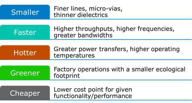
Smaller
Increased connectivity leads to the need for miniaturization and higher packing density at the PCB level. Creating challenges for PCB manufacturing and supply chains as the trend to higher packing density and thinner dielectric thickness driven by higher layer count in mechanically constrained designs affect electrical properties of the final product at PCB level.
Faster
Furthermore, as wireless data transmission bandwidth and processing speed increase the electrical performance of the PCBs laminates must improve to maintain the integrity of high-frequency signals. This is particularly challenging when considering the simultaneous reduction in packaging size and copper adhesion during interlayer layup.
Hotter
Major market segments of electronics are demonstrating trends that require more power to drive necessary performance, e.g. in networking, data centers, and automotive industry (especially for the electric vehicles market). This results in additional components (heat sinks, power conversion chips), pressure to increase board and assembly sizes, new cooling regimes (liquid cooling), and product life reduction concerns.
Greener
Future PCB factories are expected to have a smaller carbon footprint and safer chemistries.
Cheaper
The drive for lower costs manufacturing will continue and drive innovation.
Environmental
Environmental concerns continue to be pushed to the forefront as a “must have” with increased demand for a sustainable PCB supply. These concerns are considered during the design phase by PCB material, process and equipment suppliers. The following new solutions or operation of existing process and materials will be considered:
-
Environmental sustainability .
-
Product/process development for reduced ecological footprint.
-
Increase OEM requirement, in addition to government regulations.
A detailed view of the needs, gaps, challenges, and technology solutions on this topic is given here.
PCB Design and New Product Introductions
PCB design and new product introductions push the PCB manufacturing limits and require ever evolving capabilities and faster turnaround. From tighter mechanical component tolerances to BGA reduced pitches and aggressive narrowed trace and space designs for dense escape wiring and the needs for various surface finishes (e.g., electroless nickel immersion gold (ENIG) + hard Au, electroless nickel electroless palladium immersion gold (ENEPIC), electroless palladium autocatalytic gold (EPAG), direct immersion gold (DIG), etc.), the introduction of new PCB design will continue to demand more from PCB manufacturing capabilities and standard practices. Highlights to consider:
-
Tighter manufacturing process controls.
-
High quality requirements in aggressive designs.
-
Quick turnaround time (QTAT) for design verification.
Information on the drivers, needs, and challenges is currently being collected and will be published in 2027. If you are interested in being notified when this is released, please email here.
Test, Inspection and Measurement
With ever increasing artificial intelligence, augmented reality, connected factories, and robotics, PCB factories must keep pace to effectively compete in the emerging Industry 4.0 market. Automation is becoming a key component in company differentiation and efficiency.
The technology issues considered mainly fall into three categories:
-
Test, measurement, and inspection equipment evolution.
-
Data handling, testing protocols and traceability.
-
Reliability and quality controls.
A detailed view of the needs, gaps, challenges, and technology solutions for this topic is given here.
High Speed PCBs
The entire network continues to drive higher computational rates, larger caches of information that need to move quickly and self-learn all at near-instant data transfer speed.
The impact on PCB design and features are equally fast moving, resulting in
-
A need for material development and innovation that can keep pace with design demand.
-
Higher layer counts, miniaturization, and feature rich complexity.
-
Accelerated engineering and product introduction.
-
Core-to-core and layer-to-layer registration controls to limit cross talk.
A detailed view of the needs, gaps, challenges, and technology solutions for this topic is given here.
High Speed Substrates
Semiconductor density and chipset technological growth continues to quickly develop up as the data management ecosystem expands rapidly.
Substrate suppliers will need to implement advances quickly, innovate new processes and materials to keep pace with this trend. Specifically, there is demand for:
-
Aggressive miniaturization resulting in higher layer counts and density in smaller form factors.
-
Signal integrity, manufacturability, tolerance, and reliability performance demands.
A detailed view of the needs, gaps, challenges, and technology solutions for this topic is given here.
Microwave RF and mmWave PCBs
This section focuses on PCBs for analog signal transmission, reception and processing, particularly at millimeter-wave (mmWave) frequencies.
PCBs are expected to support processing of antennas, filters, amplifiers, filters, frequency conversion, phase shifters, splitters and combiners for increasing frequency bands for future networks beyond 5G-6G cellular communications.
Operations at these frequencies are demanding and result in extreme challenges in controlling feature and surface dimensions, particularly with the small skin depths at high frequencies. This section presents issues related to frequency drivers and types of circuits, thermal considerations, materials, and process accuracy and variations.
Laminates
Laminates refers to the combination of organic and inorganic, conductive and non-conductive materials that form the substrate upon which conducive patterns are formed and separated by dielectrics. These materials are processed and combined in circuit manufacturing processes to create printed circuit boards and IC substrates upon which semiconductors are packaged.
Information on Laminates presents the needs and challenges of miniaturization, yield and high-volume manufacturing, materials, processes, large packages for heterogeneous integration, thermal considerations, performance and assembly.
Optical Circuits
Information on the drivers, needs, and challenges is currently being collected and will be published in 2026. If you are interested in being notified when this is released, please email here.
Embedded Components
Two forms of embedding are commonly used:
-
Formed components, where the PCB dielectric and conductive traces are key elements themselves in the components, e.g. formed resistors, mmWave antennas, etc.
-
Embedded components where the components can be passive discretes or integrated active components.
Embedded technologies combine components, assembly and packaging processes in a single manufacturing facility and are the focus of this section.
Flexible Circuits and Flexible Hybrid Electronics
Information on the drivers, needs, and challenges is currently being collected and will be published in 2027. If you are interested in being notified when this is released, please email here.
Your Feedback
We welcome your comments and suggestions! Here is a link for your input.